When developing a new board, many problems can occur. Bare, unpopulated boards can have shorts and opens that can cause circuits not to work or software to fail once the board is populated. After assembly of components, solder bridges of poor solder joints can cause problems. Fortunately, you can employ Boundary Scan, also known as JTAG or IEEE 1149, to find problems that you can then fix.
Boundary scan, based on the IEEE 1149.x set of standards, is the structural testing of printed circuit boards and its installed components. Scan results include information on typical electric circuit faults that occur during PCB manufacturing and include bridging (short circuit) faults, opens, stuck-at faults (stuck at 0, stuck at 1), and line breaks.
JTAG testing is performed on a freshly manufactured board. Figure 1 highlights the process.
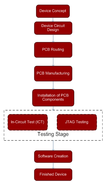
Figure 1. The testing stage consists of JTAG Boundary Scan and in-circuit testing.
JTAG testing helps detect opens in BGA (ball-grid array) packages, short circuits, breaks, as well as faulty chips with digital interfaces. It is very important to identify these defects because if an unchecked board gets into a programmer's hands, it creates problems with the launch of memory and other peripherals. It is often not clear what is wrong: programmer's settings, or installation defects. JTAG testing can identify these problems.
The testing stage (before you turn on the circuit for the first time) involves checking the board for short circuits. Then supply voltage is applied to the board and current consumption is checked, after which the main supply voltages are inspected. Then the board is either JTAG or ICT in-circuit tested (you can also run both tests at a time).
Because JTAG comes first, using it to identify problems reduces labor costs in the future. It is logical that if problems are detected after the product's assembly, it will have to be disassembled and reassembled.
The JTAG testing stage reveals:
- Opens in the PCBs with BGA packages, on which ICT testing cannot possibly be done;
- Unsoldered pull-up / pull-down resistors
- Short circuits.
You can also use JTAG technology to successfully test memory interfaces from SRAM to DDR3 (it only checks the nets integrity, not the memory). This test, combined with the flash memory test, helps send the board to the programmer to install the boot loader and the OS, as well as for subsequent bring-up (first run).
At Promwad, we've used boundary-scan software (Figure 2) to perform testing in projects with a miniature set of components, 0402 and BGA packages, high-density layouts, PCBs with more than four layers, and flexible PCBs. Let's explore the use of boundary scan in four specific projects.
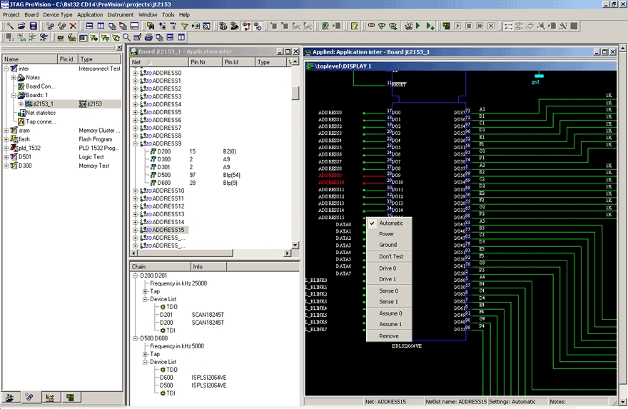
Figure 2. Boundary-scan software controls the tests and reports test results.
Case study 1: VoIP Router
Objective: Develop a VoIP telephony device based on the Blackfin BF527 processor with Linux-based software (Figure 3).
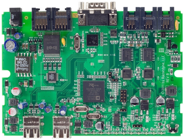
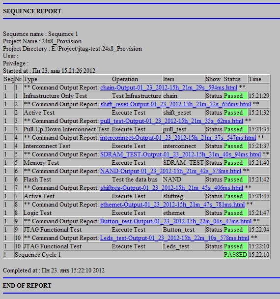
Figure 3. We performed JTAG and functional testing on this VoIP telephony card, which included SDRAM and flash memory.
The SDRAM, NAND flash memory, and Ethernet switch interface were tested under this project. We also used JTAG testing to check the correctness of LEDs and buttons, a process that involved functional tests programmed in Python, a scripting language integrated into the software. It can be used to test various digital interfaces and chips, as well as to set up flexible dialogue with the user.
The use of JTAG testing helped verify the installation and operation of the chips. Listing 1 is an example of a Python script that tests LEDs by using an SPI shift register (Figure 4). The script flashes particular LEDs and asks user if an LED turned on or off.
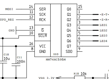
Figure 4. A Python script tested LEDs using this shift register controlled by an SPI bus.
Listing 1
#******************************************#
# Program
#******************************************#
# Write your Program here.
LED1 = 0x08
LED2=0x10
LED3=0x20
LED4=0x40

IH("DD4.J2")
register.clear()
for i in range(8):
  register.write(LED1|LED2)
  register.write(LED4|LED3)
register.write(0x78)
result=jft_outputOkNok("Leds test","Does Leds turn on?")
register.clear()

if (result == "YES"):
  sys.stderr.write("Passed")
  sys.exit(0)
else:
  sys.stderr.write("Failed")
  sys.exit(-1)
The code function register.write(BYTE) is a Python script that sends BYTE into shift register, such as a 74HC595, over the SPI bus. When the script ends, the result is "Passed" or "Failed." This result goes into the final report shown in Figure 5.
Case study 2: Plug Computer
Objective: Develop a multi-functional network device (mini-server) designed to operate in IP-based networks (Figure 6).
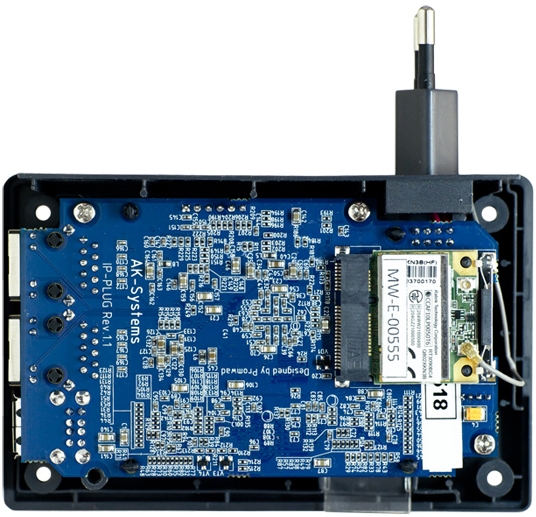
Figure 6. This embedded computer is based around the Marvell 88F6282.
This project is based on the Marvell 88F6282 CPU and DDR2 / DDR3 memory. The board had components mounted on both sids and seven chips with BGA packages. When the PCBs were soldered, memory problems were detected: the PCBs would hang up at boot time or U-boot would fail to start. Operational testing of DDR2 memory helped detect unsoldered outputs on the data bus on lines D0, D3 and D7 of one of the four memory chips. This fault caused spontaneous change of data in a specific address area.
In case of the product's versions with DDR3 memory, programmers had trouble booting Linux. Functional testing revealed that all the chips were serviceable, but the timings were wrong.
As a result, JTAG testing helped save a lot of time at the bring-up stage because when we handed the PCBs over to programmers we were confident that the memory was soldered correctly. Figure 7 shows the test report.
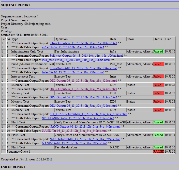
Figure 7. The test report shows a detected problem with DDR2 interface.
If you click a link, you will see a detailed report for a specific node. Figure 8 shows an excerpt from the detailed report for DDR2 interface with a detected fault (highlighted).
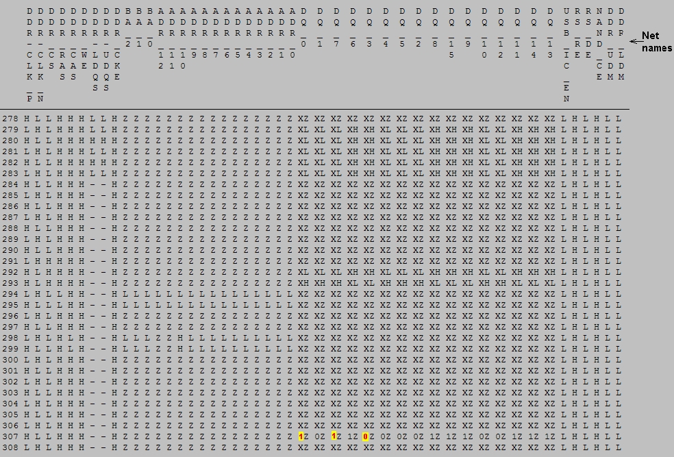
Figure 8. The detailed report of DDR2 interface testing shows the faults.
The software displays the following conditions:
- H or L – high or low level on pins, driven by JTAG (a chip with a JTAG port like CPU or MCU)
- 1 or 0 – correct value sensed from this pin
- 1 or 0 – incorrect value sensed from pin (must be the opposite)
As we see in this example, we write in a DDR2 word 0001001011010111 (lsb first), line 278 through 290. Then we read from the same place this value, but get 1000001111010111 (lsb first), line 291 through 308. It means that we have troubles with DQ0, DQ3 and DQ7. Thus, DDR chips and CPU must be removed in reinstalled, after which we can run a new round of JTAG tests.
Case study 3: Single-board computer
Objective: Develop a single-board computer for control, monitoring, and diagnostics of service equipment for trucks and special vehicles (Figure 9). The board is designed around a Fujitsu Jade graphics controller.
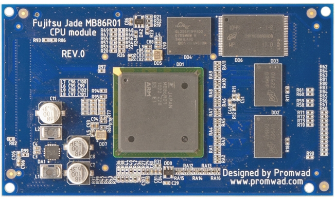
Figure 9. Boundary-scan testing helped us debug this single-board computer
This was a two-board project because it involved a CPU and a motherboard (CPU shown). The main focus was to test connections between the PCBs. The testing also involved inspection of generation in the generators, as well as the installation of NAND and NOR memory.
The testing of the product's prototypes helped detect that there was no power generation at one of the outputs. A visual inspection revealed that the generator had the wrong key.
Case study 4: A Single-board industrial computer in SODIMM form factor
Objective: Develop a special board for JTAG and functions testing and flashing of a single-board industrial computer in SODIMM factor for mass production. This device is a single-board computer (Figure 10 implemented in the SO-DIMM 200 form factor. The implementation of this project involved a detailed DFT (design-for-test) analysis (analyzed access to the TAP (test access port) controller ports, clock nets, enable signals etc.) defining the coverage and making recommendations for increasing test coverage (make clock switchable on/off by JTAG device, access to chip enable signals, etc.). To achieve maximum coverage of the PCB by JTAG testing, a special test board was designed, which increased the coverage up to 98% (only the USB interface remained uncovered because the TAP controller had no access to these outputs). Also, this bench helps flash the PCB via UART (universal asynchronous receiver transmitter) or Ethernet, as well as monitor voltages and currents.
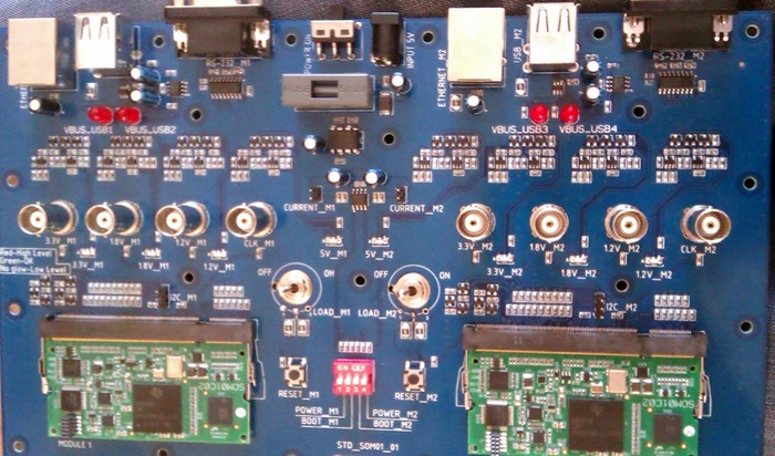
Figure 10. The test board accommodates two SO-DIMM single-board computers.
Summary
JTAG boundary scan can be successfully used at the production site to control the installation of batch-produced devices and test their prototypes. In case of mass production, JTAG testing provide us with information about quality of manufactured PCBs. It allows us to distinguish between bad and good manufacturing factories or processes. In case of PCB prototyping, JTAG tests significantly reduce time to bring up our prototype by programmers, by checking for right functionality of basic interfaces.
The advantage of JTAG testing before ICT testing is that there is no need to place additional pads for an ICT tester. Furthermore, JTAG testing can be used to test the installation of BGA enclosures, which is impossible to do with ICT (in-circuit testing).
As a result, JTAG technology can significantly reduce the prototype bring-up time. The developer writes tests in a scripting language in consideration of all the specifics of each individual circuit.