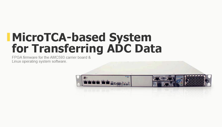

MicroTCA-based System for Transferring ADC Data
Client
A system integrator and distributor for the world's leading boards and systems manufacturers.
Challenge
To design a Vadatech’s MicroTCA-based system that transfers ADC data in blocks between FPGA and CPU and back with a defined latency. The system components are:
- MicroTCA VT855 1U;
- two FMC modules with two two-channel ADS54J60 high-speed ADCs and four-channel DAC39J84 high-speed JESD DACs;
- AMC593 сarrier board;
- AMC758 single board computer.
Solution
Concept Development
The system consists of two subsystems:
- Firmware — FPGA firmware for the AMC593 carrier board.
- Software — Linux operating system software, which includes:
- PCIe bus driver;
- high-level software for configuring the FMC231 module components;
- organization of AMC593-AMC758 communication via PCIe.
Hardware Design
The client provided us with the following hardware components for the project:
- AMC758 single-board computer with an installed Linux Fedora system;
- Two FMC modules with two two-channel ADS54J60 high-speed ADCs and four-channel DAC39J84 high-speed JESD DACs;
- AMC593 carrier board;
- Win10 laptop;
- analog signal generator and oscilloscope (Picoscope);
- MicroTCA VT855 1U.
Software Development
We designed a firmware subsystem that runs on request to collect data from the eight ADC channels and then packs and sends them over PCIe to the upstream device.
In addition, it takes data back from the upstream device via PCIe and then unpacks and transmits it to the eight DAC channels.
The software subsystem performs the following tasks:
- performs initial system initialization;
- configures and queries the Firmware;
- determines the size of PCIe exchange blocks;
- sets up the system operation modes.
There are three system operating modes:
- Loopback mode;
- Write Mode — streaming data recording mode of eight ADC channels to the file;
- Read Mode — streaming data reading from a file with the subsequent transfer to the eight DAC channels.
Let's consider the primary specifics we worked with within the project. The main difficulties in the firmware subsystem are related to packing data from 8 ADC channels and transferring to PCIe (serialize data), as well as to the subsequent reception of serial data from PCIe (deserialize data) and moving to 8 DAC channels, synchronization of data streams.
The first challenge in firmware development is to ensure the continuous transfer of the data stream to the DAC. Understanding this specificity was the most time-consuming.
The data flow from the ADC including decimation (:2000) is 64 Mb/sec, the data flow to the DAC is 358.4 Gb/sec. Thus, we need a resample module of 1:5600.
- The first method of implementing the resample module was to multiply each report 5600 times. This method turned out to be ineffective, since the analog signal was torn in phase on the oscillogram.
- The second method was the implementation of a linear interpolator with a step of 1/5600. It allowed obtaining a signal at the DAC output without phase discontinuities.
The second challenge was to develop an FSM to decompress the structures from the PCIe. A simulation of the "PCIe to JESD DAC" path was required to identify problems with data gaps between frames on the oscilloscope.
The simulation involved creating a test data stream. It simulates the data structures from PCIe; counts the number of reports received in the unpacker and the number of messages after the unpacker stacked in the buffer of each channel. When working correctly, this number stands the same.
The third difficulty was to create a mechanism for measuring the delay between data received from the ADC and transmitted to the DAC. We developed a technique, according to which the total delay was broken down into three parameters:
- static delay of the ADC path;
- static delay of the DAC tract;
- dynamic delay of the path. It includes PCIe transfer time, Linux SW processing time, driver request processing time, and data receiving time back to the FPGA.
In the firmware subsystem we have implemented dynamic delay measurement in loopback mode depending on the size of data blocks transmitted. The measured value is available in CSR address space. The requirement of TOR for delays less than 1 ms is fulfilled when the block size is not more than 512 (2 MB).
In the SW subsystem we created an application that allows us to:
- configure FMC231 module peripherals, ADC, DAC;
- activate data stream output from 8 ADC channels;
- set the size of the received/transmitted block;
- activate data streaming to 8 DAC channels;
- perform data block transmission;
- write the reports of 8 ADC channels to the file in "Write mode";
- perform cyclic data reception and transmission in "Loopback" mode;
- perform cyclic data transfer from the file to 8 DAC channels in "Read Mode".
Business Value
Our client got a ready-made system for end-to-end data collection and transmission with three operation modes.
Applied technologies:
- JESD204b;
- PCIe.
This is one of several projects that we have implemented with MTCA, an open standard for high-performance modular embedded systems. With MicroTCA, you get modularity, high scalability, and a compact design that reduces your time to market. Read more: How We Develop Custom AMC Boards and Integrate MicroTCA


